

Onto Innovation
VerifiedWebsite, address and certifications confirmed by forUdyog researchProcess control solutions across the semiconductor value chain: inspection, metrology, lithography and software.
Overview
Onto Innovation is a process control company whose portfolio spans the semiconductor value chain. Its technologies cover unpatterned wafer quality, 3D metrology from nanometer-scale transistors to large die interconnects, macro defect inspection of wafers and packages, metal interconnect composition, factory analytics, and lithography for advanced semiconductor packaging.
Its products help customers address yield, device performance, quality and reliability issues. The company is headquartered in Wilmington, Massachusetts, and supports customers through a worldwide sales and service organisation, with local support pages for China, Europe, Japan, Korea, Malaysia, Singapore, Taiwan, USA and Vietnam.
Onto also offers service programs, technical training, and a Packaging Applications Center of Excellence focused on panel-level packaging for 2.5D, FOPLP, 3D chiplet and AI packages on glass and organic substrates.
Products
9 listedVideos
Catalogues & brochures
Certifications
1 listedAs stated by the company
- ISO 9001:2015Source
Factory & locations
Onto Innovation
VerifiedProcess control solutions across the semiconductor value chain: inspection, metrology, lithography and software.
Overview
Onto Innovation is a process control company whose portfolio spans the semiconductor value chain. Its technologies cover unpatterned wafer quality, 3D metrology from nanometer-scale transistors to large die interconnects, macro defect inspection of wafers and packages, metal interconnect composition, factory analytics, and lithography for advanced semiconductor packaging.
Its products help customers address yield, device performance, quality and reliability issues. The company is headquartered in Wilmington, Massachusetts, and supports customers through a worldwide sales and service organisation, with local support pages for China, Europe, Japan, Korea, Malaysia, Singapore, Taiwan, USA and Vietnam.
Onto also offers service programs, technical training, and a Packaging Applications Center of Excellence focused on panel-level packaging for 2.5D, FOPLP, 3D chiplet and AI packages on glass and organic substrates.
- Headquarters
- Wilmington, Massachusetts, USA
- Product families
- 4Di, Aspect, Atlas, Discover, Dragonfly, Element, FAaST, IMPULSE, Iris, IVS, JetStep, PrimaScan
- Market segments
- Wafer & panel manufacturing, CMOS, specialty, advanced packaging, industrial
Products
 Dragonfly® G5 System2D inspection3D metrologyIR imaging
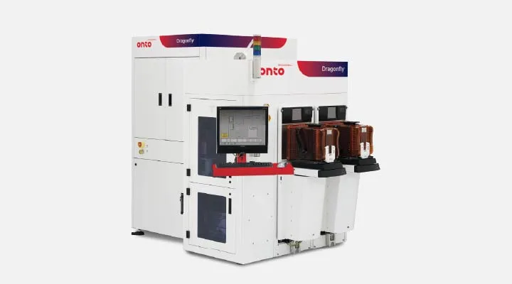 Dragonfly® G3 System2D inspection3D metrology
 Iris™ S System150/200/300mm wafersFilm metrologyOCD
 IMPULSE® V SystemCMP metrologyAI analytics
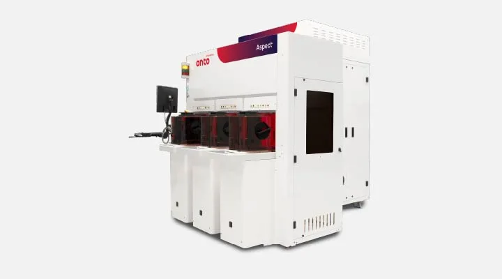 Aspect® SystemIRCDNon-destructiveIn-line
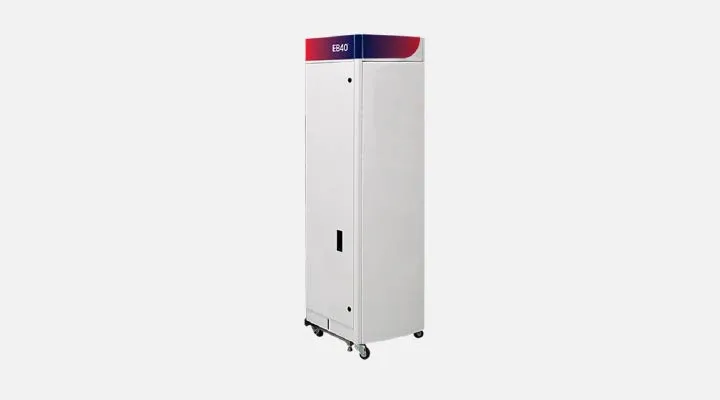 EB40™ ModuleEdge inspectionBackside inspection
 Discover® Defect SoftwareDefect managementSoftware
 TrueADC® SoftwareDeep learningADCSoftware
- Advanced packaging lithography steppersStepperPanel-level
Contact
Phone, e-mail, WhatsApp, website and the point of contact are free for every supplier in Machinery & Suppliers.